PCB Soldering-15 Common PCB Soldering Problems to Avoid
By understanding the 15 common PCB soldering problems discussed in this article and implementing the recommended preventive measures, you can significantly improve the quality of
Solder Pads: Complete Guide to PCB Pad Design & Types
Oversized pads may cause excessive solder spreading, bridging between adjacent pads, or tombstoning of small components. Undersized pads can lead to insufficient solder joints, poor electrical contact, or
How are the PCB solderability deteriorated?
If the solder paste is too old or has been exposed to excessive heat or moisture, it may not flow properly during reflow, resulting in poor bonding with the pad.

What Is a Solder Pad? Full Guide to PCB Pad Design
Solder pad lifting or damage can occur due to excessive heat, poor soldering techniques, or mechanical stress. It can also happen if the pad is too small or if the PCB''s copper plating is
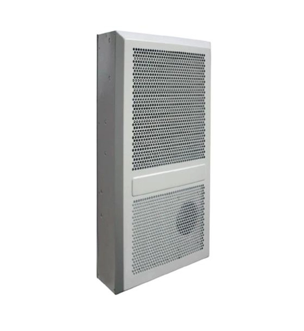
Supply Chain Resilience for Optical Modules: Failure Analysis
Why Supply Chain Resilience for Optical Modules Fails at Hyperscale The industry-standard approach—maintaining an approved vendor list (AVL) and relying on compliance testing for
Why Solder Pad Design Matters: Key to Reliable Solder
Excess solder paste can cause "solder bridging" between adjacent pins. It can also cause the component to float or "skew" during reflow, leading to misalignment. A
Why does your pcb keep having solder pick-off?An Ultimate guide to
Remember, in electronics manufacturing, the devil is in the details. Only by maintaining meticulous attention to every step can you end the nightmare of poor soldering on your PCB,
Why does your pcb keep having solder pick-off?An
Remember, in electronics manufacturing, the devil is in the details. Only by maintaining meticulous attention to every step can you end the nightmare
Pad Contamination on a Printed Circuit Board
It is worth pointing out that during wave soldering the resist on the pad may affect the visual appearance of the joints but it will not cause any problems of reliability.
Under the Microscope: Identifying Common PCB Contaminants and
These contaminants can interfere with soldering quality or create conductive paths if not cleaned properly. This is why cleanroom protocols and gloves are often recommended during
Understanding Solder Joint Failure in PCB Manufacturing
Learn and discover the reasons behind solder joint failure, how it affects PCB reliability, and methods to detect it early.
PCB Pad in PCB Design & Development: Solder Pads Explained
The pad layout must precisely match the component package dimensions and appropriately sized pads help prevent soldering defects such as tombstoning and solder bridging.
LGA solder pad problem
On pads under a package there''s nowhere for excess solder to go and it can physically hold the package up in the air and prevent other pads soldering properly. Check the manufacturers
Optical Power Meters & Sources
High-precision power meters (Ge/InGaAs) and stabilized light sources for insertion loss and return loss testing.
OTDR & Fiber Characterization
Full-featured OTDR, fiber OTDR testers, and modular OTDR test modules for network deployment and troubleshooting.
OSA & Eye Diagram Analyzer
High-resolution OSA for DWDM and eye diagram testers for signal integrity validation.
BERT & Endface Inspection
BERT up to 800G, fiber endface inspection probes, and extinction ratio meters for comprehensive testing.