Co-packaged optics (CPO): status, challenges, and solutions
Co-packaged optics (CPO) is a disruptive approach to increasing the interconnecting bandwidth density and energy efficiency by dramatically shortening the electrical link length through advanced

Optical Interconnects and Packaging 2026
This paper presents the development of wafer-level optical coupling packaging techniques that enable optoelectronic surface emitting or receiving components with passive and
Optical Packaging and Interconnection
This paper discusses the drivers for optoelectronic devices and optical PWBs, the major differences between IC packaging and optoelectronic device packaging, the emerging evolution of optical printed
Optical Transceiver: Packaging Methods & Optical Chip Types
For the design and manufacturing of fiber optic transceivers, the choice of packaging methods and optical chip types is one of the key factors. This article analyzes the requirements of...
Advanced Packaging Evolution: Chiplet and Silicon Photonics-CPO
In the long run, we believe the ideal packaging solution will involve utilizing a full-scale wafer as a single packaged device. To achieve ExaFLOPS computing power, it requires at least 1,000 AI chiplets
Photonic Integrated Circuits: Research Advances and Challenges in
This review focuses specifically on the optical interconnection and packaging technologies for photonic chips.
Researching | Study on Active Optoelectronic Device Packaging
The technical approaches and reliability of the active optoelectronic devices were studied, including coaxial and box-type package structure, electrical and optical parts attachment materials and fiber
Optical Packaging/Module Technologies: Design Methodologies
Achieving high performance in the module requires not only the chip design, but also requires the package design, which includes optical, electrical, mechanical, and thermal designs. The chapter
Photonic Integrated Circuits: Research Advances and
This review focuses specifically on the optical interconnection and packaging technologies for photonic chips.
Optical Interconnects and Packaging 2025
SPIE uses a seven-digit CID article numbering system structured as follows: The first five digits correspond to the SPIE volume number. The last two digits indicate publication order within the
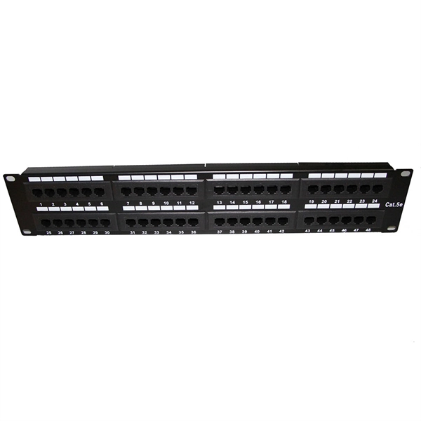
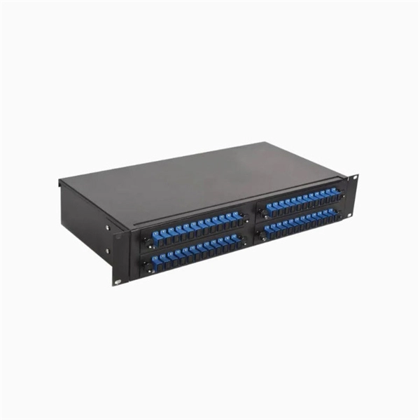
Optical device packaging technology: COB,BOX and coaxial
Common optical device packaging methods include COB (chip-on-board packaging), BOX and coaxial packaging. Today, we will discuss the differences between them to help you better
LED and Optical Device Packaging and Materials
The first section will review materials challenges and some solutions for the packaging of high power LEDs, followed by functions of packaging and materials for advanced optoelectronic device
Advanced optical packaging – how much do you know ?
In this article, I will systematically introduce optical packaging, its importance, and its associated aspects. Optical transceiver modules can be
Packaging multiple active and passive elements in a hybrid optical
Two novel approaches to optical packaging have been developed: a localized laser soldering process and a flexure-based lens mount with large dynamic range. We present the optical
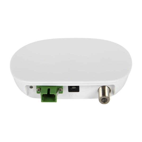
Optical Power Meters & Sources
High-precision power meters (Ge/InGaAs) and stabilized light sources for insertion loss and return loss testing.
OTDR & Fiber Characterization
Full-featured OTDR, fiber OTDR testers, and modular OTDR test modules for network deployment and troubleshooting.
OSA & Eye Diagram Analyzer
High-resolution OSA for DWDM and eye diagram testers for signal integrity validation.
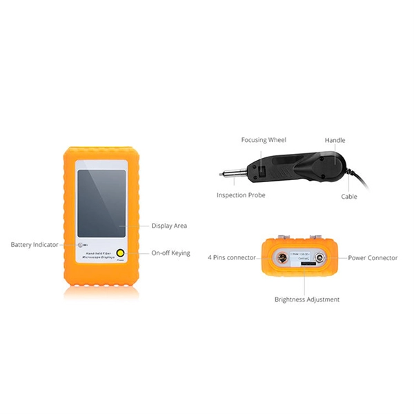
BERT & Endface Inspection
BERT up to 800G, fiber endface inspection probes, and extinction ratio meters for comprehensive testing.